


IIS-BUS INTERFACE S3C2410A
21-2
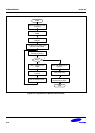
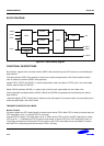
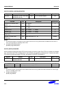
BLOCK DIAGRAM
ADDR
DATA
CNTL
PCLK
BRFC
IPSR_A
IPSR_B
TxFIFO
RxFIFO
SCLKG
CHNC
SFTR
LRCK
SCLK
SD
CDCLK
Figure 21-1. IIS-Bus Block Diagram
FUNCTIONAL DESCRIPTIONS
Bus interface, register bank, and state machine (BRFC): Bus interface logic and FIFO access are controlled by the
state machine.
5-bit dual prescaler (IPSR): One prescaler is used as the master clock generator of the IIS bus interface and the
other is used as the external CODEC clock generator.
64-byte FIFOs (TxFIFO and RxFIFO): In transmit data transfer, data are written to TxFIFO, and, in the receive data
transfer, data are read from RxFIFO.
Master IISCLK generator (SCLKG): In master mode, serial bit clock is generated from the master clock.
Channel generator and state machine (CHNC): IISCLK and IISLRCK are generated and controlled by the channel
state machine.
16-bit shift register (SFTR): Parallel data is shifted to serial data output in the transmit mode, and serial data input is
shifted to parallel data in the receive mode.
TRANSMIT OR RECEIVE ONLY MODE
Normal Transfer
IIS control register has FIFO ready flag bits for transmit and receive FIFOs. When FIFO is ready to transmit data, the
FIFO ready flag is set to '1' if transmit FIFO is not empty.
If transmit FIFO is empty, FIFO ready flag is set to '0'. When receive FIFO is not full, the FIFO ready flag for receive
FIFO is set to '1' ; it indicates that FIFO is ready to receive data. If receive FIFO is full, FIFO ready flag is set to '0'.
These flags can determine the time that CPU is to write or read FIFOs. Serial data can be transmitted or received
while the CPU is accessing transmit and receive FIFOs in this way.