


S3C2410A I/O PORTS
9-21
DCLK CONTROL REGISTERS (DCLKCON)
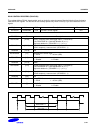
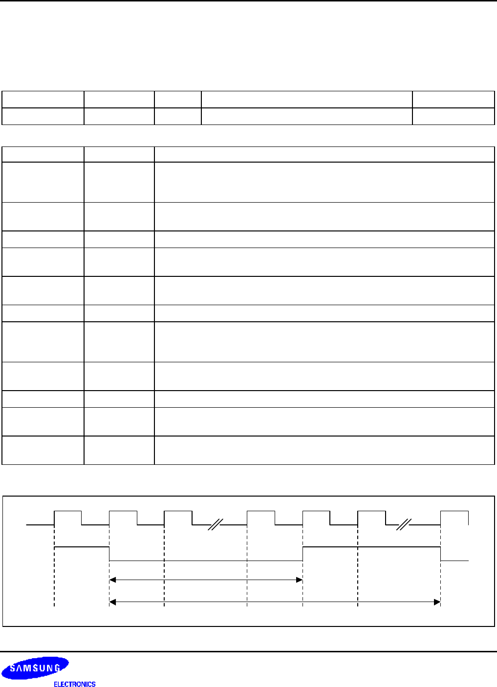
This register defines DCLKn signals, which work as clocks for external sources. See the following figure for how to
make the DCLKn signals. The DCLKCON can actually operate only when CLKOUT[1:0] is set to send the DCLKn
signals.
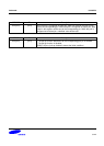
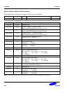
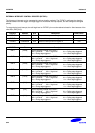
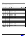
Register Address R/W Description Reset Value
DCLKCON 0x56000084 R/W DCLK0/1 control register 0x0
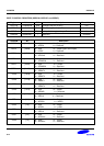
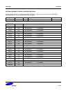
DCLKCON Bit Description
DCLK1CMP [27:24] DCLK1 Compare value clock toggle value. (< DCLK1DIV)
If the DCLK1CMP is n, Low level duration is (n + 1).
High level duration is ( (DCLK1DIV + 1) – (n +1) ).
DCLK1DIV [23:20] DCLK1 Divide value
DCLK1 frequency = source clock / (DCLK1DIV + 1)
Reserved [19:18] 00b
DCLK1SelCK [17] Select DCLK1 source clock
0 = PCLK 1 = UCLK (USB)
DCLK1EN [16] DCLK1 Enable
0 = Disable 1 = Enable
Reserved [15:12] 0000b
DCLK0CMP [11:8] DCLK0 Compare value clock toggle value. (< DCLK0DIV)
If the DCLK0CMP is n, Low level duration is (n + 1).
High level duration is ( (DCLK0DIV + 1) – (n +1) ).
DCLK0DIV [7:4] DCLK0 Divide value.
DCLK0 frequency = source clock / (DCLK0DIV + 1)
Reserved [3:2] 00b
DCLK0SelCK [1] Select DCLK0 source clock
0 = PCLK 1 = UCLK (USB)
DCLK0EN [0] DCLK0 Enable
0 = Disable 1 = Enable
DCLKnDIV + 1
DCLKnCMP + 1