S3C2410A PRODUCT OVERVIEW
1-5
BLOCK DIAGRAM
ARM920T
ARM9TDMI
Processor core
(Internal Embedded ICE)
DD[31:0]
WriteBack
PA Tag
RAM
Data
MMU
C13
DVA[31:0]DV A[31:0]
Instruction
CACHE
(16KB)
Instruction
MMU
External
Coproc
Interface
C13
ID[31:0]
IPA[31:0]
IV A[31:0]
CP15
Write
Buffer
AMBA
Bus
I/F
JTAG
Data
CACHE
(16KB)
WBPA[31:0]
DPA[31:0]
Bridge & DMA (4Ch)
Clock Generator
(M PLL)
A
H
B
B
U
S Memory CONT.
SRAM/NOR/SDRAM
BUS CONT.
Arbitor/Decode
Power
Management
Interrupt CONT.USB Host CONT.
ExtMaster
LCD
DMA
LCD
CONT.
A
P
B
B
U
S
I2C
GPIO
I2S
RTC
SPI
ADC
SDI/MMC
USB Device
Watchdog
Timer
BUS CONT.
Arbitor/Decode
Timer/PWM
0 ~ 3, 4(Internal)
SPI 0, 1
UART 0, 1, 2
NAND CONT.
NAND Flash Boot
Loader
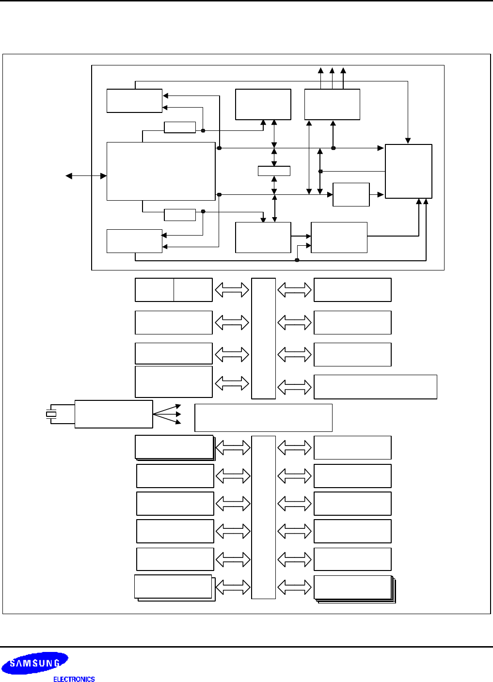
Figure 1-1. S3C2410A Block Diagram


