


MMU ARM920T PROCESSOR
3-4
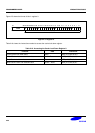
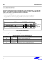
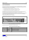
All the CP15 MMU registers, except register 8, contain state and can be read using MRC instructions and written
using MCR instructions. Registers 5 and 6 are also written by the MMU during a data abort. Writing to Register 8
causes the MMU to perform a TLB operation, to manipulate TLB entries. This register cannot be read. The instruction
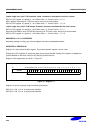
TLB (I TLB) and data TLB (D TLB) both have a copy of register 10, the opcode_2 field in the CP15 instruction is used
to determine which one is accessed.
The system control coprocessor (CP15) is described in Programmer's Model on page 2-1. Details of register format
and the coprocessor instructions to access them are given there.
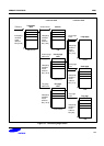
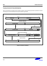
ADDRESS TRANSLATION
The MMU translates virtual addresses generated by the CPU core (and by CP15 register 13) into physical addresses
to access external memory. It also derives and checks the access permission, using a translation lookaside buffer
(TLB).
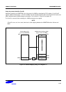
The MMU table walking hardware is used to add entries to the TLB. The translation information, which comprises
both the address translation data and the access permission data, resides in a translation table located in physical
memory. The MMU provides the logic needed to traverse this translation table and load entries into the TLB.
There are up to two stages to the hardware table walking (and hence permission checking) process. The number of
stages depends on whether the address in question has been marked as a section-mapped access or a page-
mapped access. There is one size of section and three sizes of page-mapped access (large pages, small pages and
tiny pages). The translation process always starts out in the same way, with a level one fetch. A section-mapped
access requires only a level one fetch, but a page-mapped access requires a subsequent level two fetch.