ADC AND TOUCH SCREEN INTERFACE S3C2410A
16-2
ADC & TOUCH SCREEN INTERFACE OPERATION
BLOCK DIAGRAM
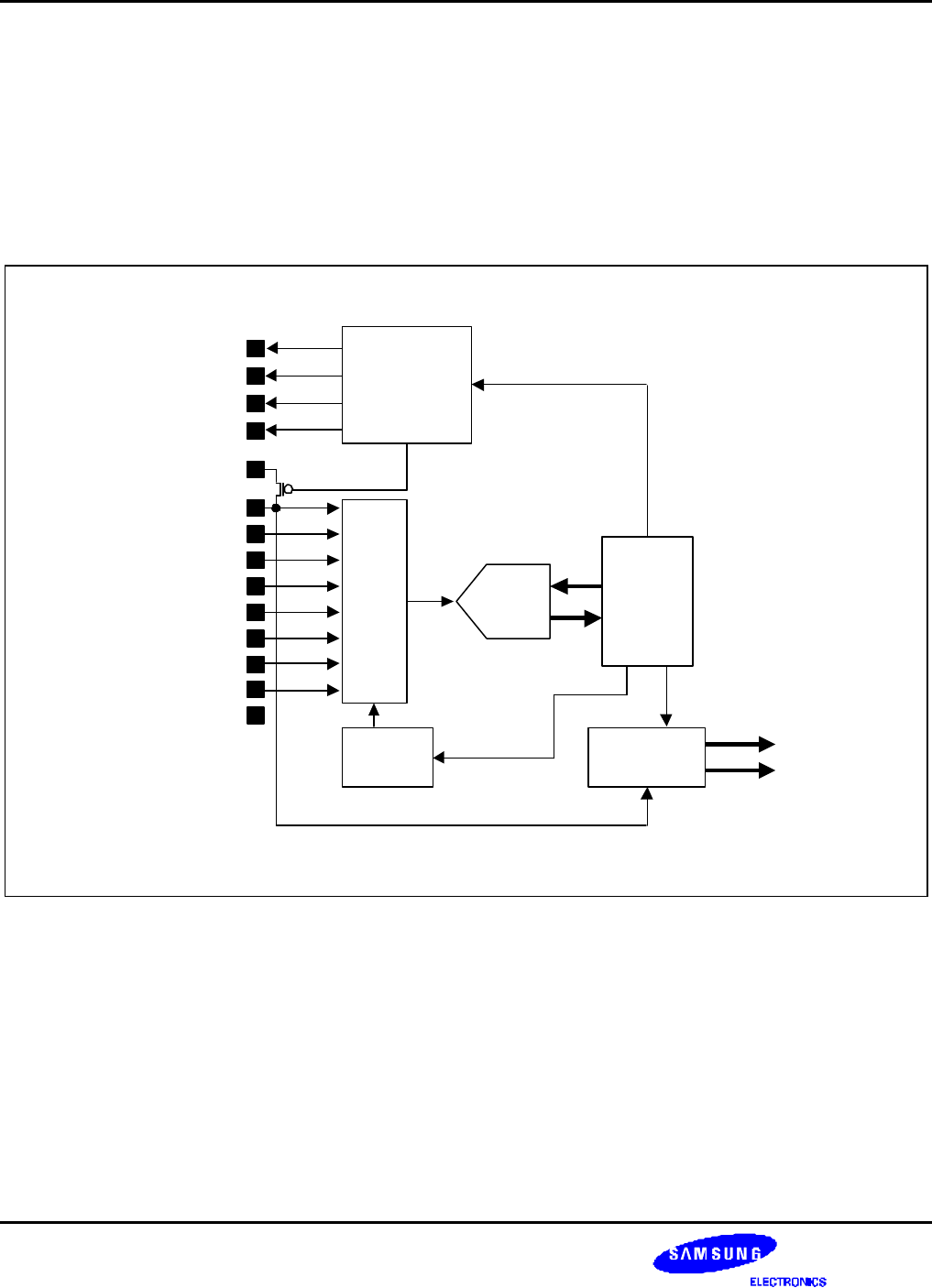
Figure 16-1 shows the functional block diagram of the S3C2410A A/D converter and Touch Screen Interface. Note
that the A/D converter is a recycling type.
A pull-up resister is attached to AIN[7] on VDDA_ADC. So, XP pad of the touch screen panel should be connected
with AIN[7] of the S3C2410A and YP pad of the touch screen panel should be connected with AIN[5].
EINT[23]
External
Transistor
Control
A/D
Convert
EINT[22]
EINT[21]
EINT[20]
VDDA_ADC
VSSA_ADC
nYPON
YMON
nXPON
XMON
8:1
MUX
ADC Input
Control
Waiting for Interrupt Mode
Interrupt
Generation
ADC
Interface
&Touch
Screen
Controller
INT_ADC
INT_TC
AIN[7]
AIN[6]
AIN[5]
AIN[4]
AIN[3]
AIN[2]
AIN[1]
AIN[0]
Figure 16-1. ADC and Touch Screen Interface Block Diagram


