


PRODUCT OVERVIEW S3C2410A
1-20
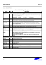
SIGNAL DESCRIPTIONS
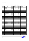
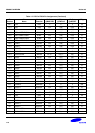
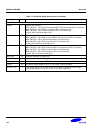
Table 1-3. S3C2410A Signal Descriptions
Signal I/O Descriptions
Bus Controller
OM [1:0] I OM [1:0] sets S3C2410A in the TEST mode, which is used only at fabrication. Also, it
determines the bus width of nGCS0. The pull-up/down resistor determines the logic
level during the RESET cycle.
00:Nand-boot 01:16-bit 10:32-bit 11:Test mode
ADDR [26:0] O ADDR [26:0] (Address Bus) outputs the memory address of the corresponding bank.
DATA [31:0] IO DATA [31:0] (Data Bus) inputs data during memory read and outputs data during
memory write. The bus width is programmable among 8/16/32-bit.
nGCS [7:0] O nGCS [7:0] (General Chip Select) are activated when the address of a memory is
within the address region of each bank. The number of access cycles and the bank
size can be programmed.
nWE O nWE (Write Enable) indicates that the current bus cycle is a write cycle.
nOE O nOE (Output Enable) indicates that the current bus cycle is a read cycle.
nXBREQ I nXBREQ (Bus Hold Request) allows another bus master to request control of the local
bus. BACK active indicates that bus control has been granted.
nXBACK O nXBACK (Bus Hold Acknowledge) indicates that the S3C2410A has surrendered
control of the local bus to another bus master.
nWAIT I nWAIT requests to prolong a current bus cycle. As long as nWAIT is L, the current
bus cycle cannot be completed.
If nWAIT signal isn't used in your system, nWAIT signal must be tied on pull-up
resistor.
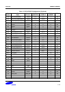
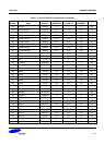
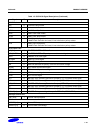
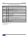
SDRAM/SRAM
nSRAS O SDRAM Row Address Strobe
nSCAS O SDRAM Column Address Strobe
nSCS [1:0] O SDRAM Chip Select
DQM [3:0] O SDRAM Data Mask
SCLK [1:0] O SDRAM Clock
SCKE O SDRAM Clock Enable
nBE [3:0] O Upper Byte/Lower Byte Enable (In case of 16-bit SRAM)
nWBE [3:0] O Write Byte Enable