


ARM920T PROCESSOR PROGRAMMER'S MODEL
2-5
ACCESSING CP15 REGISTERS
Throughout this section the following terms and abbreviations are used.
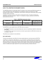
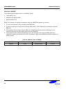
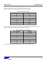
Table 2-3. CP15 Abbreviations
Term Abbreviation Description
Unpredictable UNP For reads, the data returned when reading from this location is
unpredictable; it could have any value.
For writes, writing to this location will cause unpredictable behavior, or
an unpredictable change in device configuration.
Should be zero SBZ When writing to this location, all bits of this field should be 0.
In all cases, reading from, or writing any data values to any CP15 registers, including those fields specified as
unpredictable or should be zero, will not cause any permanent damage.
All CP15 register bits that are defined and contain state, are set to zero by BnRES except V-Bit in register 1, which
takes the value of macrocell input VINITHI when BnRES is asserted.
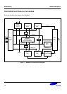
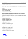
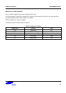
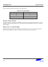
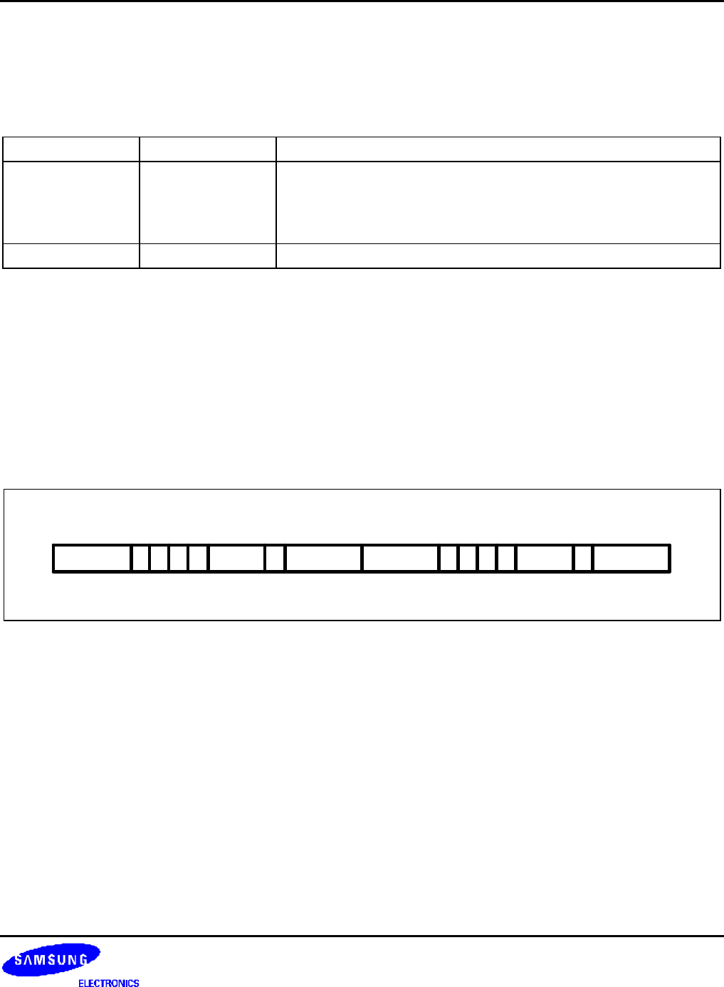
CP15 registers can only be accessed with MRC and MCR instructions in a privileged mode. The instruction bit
pattern of the MCR and MRC instructions is shown in Figure 2-1. The assembler for these instructions is
MCR/MRC{cond} P15,opcode_1,Rd,CRn,CRm,opcode_2
31 27 19 1528 16 111221 20
L CRn Rd opcode2 1 CRm
8 7 4 3 0
1 1 1 1opcode1111 0Cond
26 25 24 23 10 9 5
Figure 2-1. CP15 MRC and MCR Bit Pattern
Instructions CDP, LDC and STC, along with unprivileged MRC and MCR instructions to CP15 will cause the
undefined instruction trap to be taken. The CRn field of MRC and MCR instructions specifies the coprocessor register
to access. The CRm field and opcode_2 field are used to specify a particular action when addressing registers.
Attempting to read from a non-readable register, or writing to a non-writable register will cause unpredictable results.
The opcode_1, opcode_2 and CRm fields should be zero, except when the values specified are used to select the
desired operations, in all instructions which access CP15. Using other values will result in unpredictable behavior.