


ARM920T PROCESSOR PROGRAMMER'S MODEL
2-11
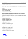
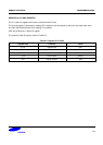
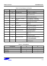
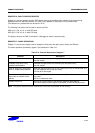
Table 2-10. Control Register 1-bit Functions
Register Bits Name Function Value
31 iA bit Asynchronous clock select See Table 2-11 on page 2-11.
30 nF bit notFastBus select See Table 2-11 on page 2-11.
29:15 – Reserved Read = Unpredictable
Write = Should be zero
14 RR bit Round robin replacement 0 = Random replacement
1 = Round robin replacement
13 V bit Base location of exception
registers
0 = Low addresses = 0x0000 0000
1 = High addresses = 0xFFFF 0000
12 I bit Instruction cache enable 0 = Instruction cache disabled
1 = Instruction cache enabled
11:10 – Reserved Read = 00
Write = 00
9 R bit ROM protection This bit modifies the MMU protection system.
See Table 3-6 on page 3-20
8 S bit System protection This bit modifies the MMU protection system.
See Table 3-6 on page 3-20
7 B bit Big-endian/little-endian 0 = Little-endian operation
1 = Big-endian operation
6:3 – Reserved Read = 1111
Write = 1111
2 C bit Data cache enable 0 = Data cache disabled
1 = Data cache enabled
1 A bit Alignment fault enable Data address alignment fault checing.
0 = Fault checking disabled
1 = Fault checking enabled
0 M bit MMU enable 0 = MMU disabled
1 = MMU enabled
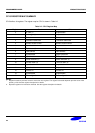
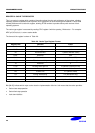
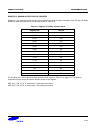
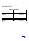
Register 1 bits 31:30 select the clocking mode of the ARM920T, as shown in Table 2-11.
Table 2-11. Clocking Modes
Clocking Mode iA nF
FastBus mode 0 0
Reserved 1 0
Synchronous 0 1
Asynchronous 1 1