


PRODUCT OVERVIEW S3C2410A
1-22
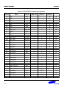
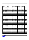
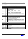
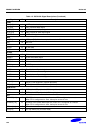
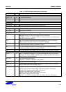
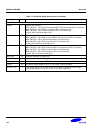
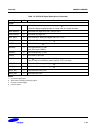
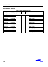
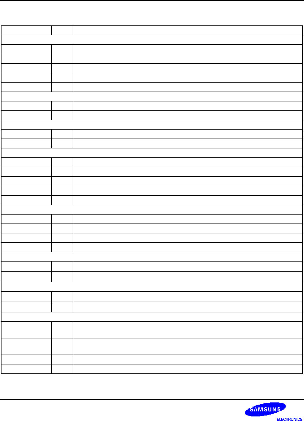
Table 1-3. S3C2410A Signal Descriptions (Continued)
Signal I/O Descriptions
UART
RxD [2:0] I UART receives data input
TxD [2:0] O UART transmits data output
nCTS [1:0] I UART clear to send input signal
nRTS [1:0] O UART request to send output signal
UEXTCLK I UART clock signal
ADC
AIN [7:0] AI ADC input [7:0]. If it isn't used pin, it has to be in Ground.
Vref AI ADC Vref
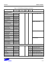
IIC-Bus
IICSDA IO IIC-bus data
IICSCL IO IIC-bus clock
IIS-Bus
I2SLRCK IO IIS-bus channel select clock
I2SSDO O IIS-bus serial data output
I2SSDI I IIS-bus serial data input
I2SSCLK IO IIS-bus serial clock
CDCLK O CODEC system clock
Touch Screen
nXPON O Plus X-axis on-off control signal
XMON O Minus X-axis on-off control signal
nYPON O Plus Y-axis on-off control signal
YMON O Minus Y-axis on-off control signal
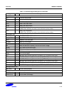
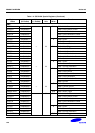
USB Host
DN [1:0] IO
DATA (–) from USB host. (15Kohm pull-down)
DP [1:0] IO
DATA (+) from USB host. (15Kohm pull-down)
USB Device
PDN0 IO
DATA (–) for USB peripheral. (470Kohm pull-down)
PDP0 IO
DATA (+) for USB peripheral. (1.5Kohm pull-up)
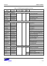
SPI
SPIMISO [1:0] IO SPIMISO is the master data input line, when SPI is configured as a master.
When SPI is configured as a slave, these pins reverse its role.
SPIMOSI [1:0] IO SPIMOSI is the master data output line, when SPI is configured as a master.
When SPI is configured as a slave, these pins reverse its role.
SPICLK [1:0] IO SPI clock
nSS [1:0] I SPI chip select (only for slave mode)