


LCD CONTROLLER S3C2410A
15-28
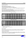
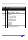
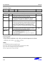
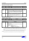
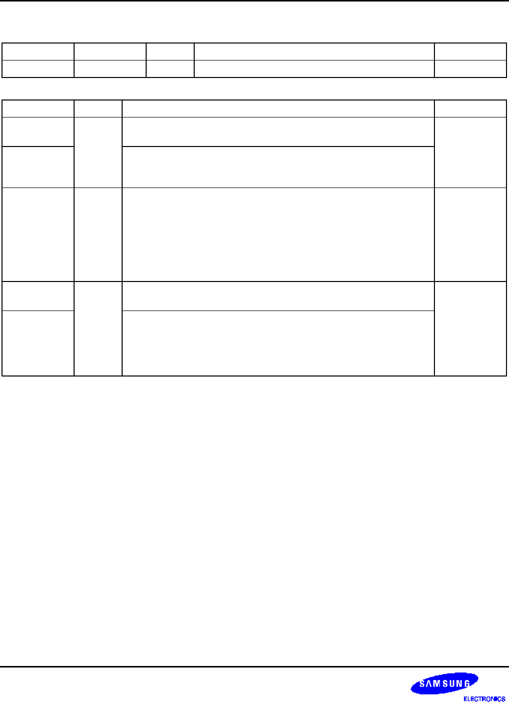
LCD Control 3 Register
Register Address R/W Description Reset Value
LCDCON3 0X4D000008 R/W LCD control 3 register 0x00000000
LCDCON3 Bit Description Initial state
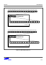
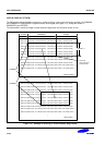
HBPD (TFT) [25:19] TFT: Horizontal back porch is the number of VCLK periods between
the falling edge of HSYNC and the start of active data.
0000000
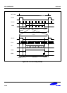
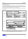
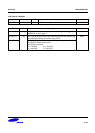
WDLY (STN) STN: WDLY[1:0] bits determine the delay between VLINE and VCLK
by counting the number of the HCLK. WDLY[7:2] are reserved.
00 = 16 HCLK, 01 = 32 HCLK, 10 = 48 HCLK, 11 = 64 HCLK
HOZVAL [18:8] TFT/STN: These bits determine the horizontal size of LCD panel.
HOZVAL has to be determined to meet the condition that total bytes
of 1 line are 4n bytes. If the x size of LCD is 120 dot in mono mode,
x=120 cannot be supported because 1 line consists of 15 bytes.
Instead, x=128 in mono mode can be supported because 1 line is
composed of 16 bytes (4n). LCD panel driver will discard the additional
8 dot.
00000000000
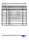
HFPD (TFT) [7:0] TFT: Horizontal front porch is the number of VCLK periods between
the end of active data and the rising edge of HSYNC.
0X00
LINEBLANK
(STN)
STN: These bits indicate the blank time in one horizontal line duration
time. These bits adjust the rate of the VLINE finely.
The unit of LINEBLANK is HCLK X 8.
Ex) If the value of LINEBLANK is 10, the blank time is inserted to
VCLK during 80 HCLK.
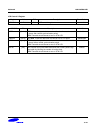
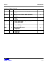
Programming NOTE
: In case of STN LCD, (LINEBLANK + WLH + WDLY) value should be bigger than (14+12xTmax).
(LINEBLANK + WLH + WDLY) = (14 + 8xTmax1 + 4xTmax2)
= (14 + 12xTmax)
LEGEND:
(1) 14: SDRAM Auto refresh bus acquisition cycles
(2) 8x Tmax1: Cache fill cycle X the Slowest Memory access time (Ex, ROM)
(3) 4x Tmax2: 0xC~0xE address Frame memory Access time
(4) Tmax: Large one of the Tmax1 and Tmax2.