


CACHES, WRITE BUFFER ARM920T PROCESSOR
4-8
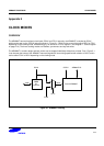
A linefill performs an 8-word burst read from the ASB and places it as a new entry in the cache, possible replacing
another line at the same location within the cache. The location which is replaced (called the victim) is chosen from
the entries which are not locked using either a random or round-robin replacement policy. If the cache line being
replaced is marked as dirty, indicating that it has been modified and that main memory has not been updated to
reflect the change, a cache writeback occurs.
Depending on whether one or both halves of the cache line are dirty, the writeback will perform a 4 or 8-word
sequential burst write access on the ASB. The writeback data is placed in the write buffer and then the linefill data is
read from the ASB. The CPU can the continue while the writeback data is written to memory via the ASB.
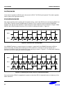
Load multiple (LDM) instructions accessing NCNB or NCB regions perform sequential bursts on the ASB. Store
multiple (STM) instructions accessing NCNB regions also perform sequential bursts on the ASB.
The sequential burst will be split into two bursts if it crosses a 1KB boundary. This is because the smallest MMU
protection and mapping size is 1KB, so the memory regions on each size of the 1KB boundary may have different
properties.
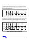
This means that no sequential access generated by ARM920T will cross a 1KB boundary, which can be exploited to
simplify memory interface design. For example, a simple page mode DRAM controller could perform a page-mode
access for each sequential access, provided the DRAM page size is 1KB or larger.
See also Cache coherence on page 4-10.
DATA CACHE REPLACEMENT ALGORITHM
The DCache and ICache replacement algorithm is selected by the RR bit in the CP15 Control register (CP15 register
1, bit 14). Random replacement is selected at reset. Setting the RR bit to 1 selects round-robin replacement.
SWAP INSTRUCTIONS
Swap instruction (SWP or SWPB) behavior is dependent on whether the memory region is cacheable or non-
cacheable.
Swap instructions to cacheable regions of memory are useful for implementing semaphores or other synchronization
primitives in multithreaded uniprocessor software systems.
Swap instructions to non-cacheable memory regions are useful for synchronization between two bus masters in a
multi-master bus system. This could be two processors, or a processor and a DMA controller.
When a swap instruction accesses a cacheable region of memory (WT or WB), the DCache and write buffer behavior
will be the same as having a load followed by a store according to the normal rules described. The BLOK pin will not
be asserted during the execution of the instruction. It is guaranteed that no interrupt can occur between the load and
store portions of the swap.
When a swap instruction accesses a non-cacheable (NCB or NCNB) region of memory, the write buffer is drained,
and a single word or byte will be read from the ASB. The write portion of the swap will then be treated as non-
bufferable, regardless of the value of Btt, and the processor stalled until the write is completed on the ASB. The
BLOK pin will be asserted to indicate that the read and write should be treated as an atomic operation on the bus.
Like all other data accesses, a swap to a non-cacheable region which hits in the cache indicates a programming
error.