


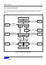

ARM920T PROCESSOR MMU
3-25
INTERACTION OF THE MMU AND CACHES
The MMU is enabled and disabled using bit 0 of the CP15 control register.
ENABLING THE MMU
To enable the MMU:
1) Program the translation table base and domain access control registers.
2) Program level 1 and level 2 page tables as required.
3) Enable the MMU by setting bit 0 in the control register.
Care must be taken if the translated address differs from the untranslated address as several instructions following
the enabling of the MMU may have been prefetched with the MMU off (using physical = virtual address - flat
translation) and enabling the MMU may be considered as a branch with delayed execution. A similar situation
occurs when the MMU is disabled. Consider the following code sequence:
MRC p15, 0, R1, c1, C0, 0: Read control rejection
ORR R1, #0x1
MCR p15,0,R1,C1, C0,0 ; Enable MMUS
Fetch Flat
Fetch Flat
Fetch Translated
The instruction and data caches can be enabled simultaneously with the MMU using a single MCR instruction.
DISABLING THE MMU
To disable the MMU, clear bit 0 in the control register. The data cache should be disabled prior to, or, at the same
time as the MMU is disabled by clearing Bit 2 of the control register. See the paragraph in Enabling the MMU
regarding prefetch effects.
NOTE
If the MMU is enabled, then disabled and subsequently re-enabled the contents of the TLBs will have been
preserved. If these are now invalid, the TLBs should be invalidated before the MMU is re-enabled. See
Register 8: TLB operations on page 2-18.