


S3C2410A SPI INTERFACE
22-3
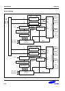
SPI OPERATION
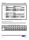
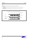
Using the SPI interface, the S3C2410A can send/receive 8 –bit data simultaneously with an external device. A serial
clock line is synchronized with the two data lines for shifting and sampling of the information. When the SPI is the
master, transmission frequency can be controlled by setting the appropriate bit to SPPREn register. You can modify
its frequency to adjust the baud rate data register value. When the SPI is a slave, other master supplies the clock.
When the programmer writes byte data to SPTDATn register, SPI transmit/receive operation will start
simultaneously. In some cases, nSS should be activated before writing byte data to SPTDATn.
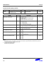
Programming Procedure
When a byte data is written into the SPTDATn register, SPI starts to transmit if ENSCK and MSTR of SPCONn
register are set. You can use a typical programming procedure to operate an SPI card.
To program the SPI modules, follow these basic steps:
1. Set Baud Rate Prescaler Register (SPPREn).
2. Set SPCONn to configure properly the SPI module.
3. Write data 0xFF to SPTDATn 10 times in order to initialize MMC or SD card.
4. Set a GPIO pin, which acts as nSS, to low to activate the MMC or SD card.
5. Tx data → Check the status of Transfer Ready flag (REDY = 1), and then write data to SPTDATn.
6. Rx data(1): SPCONn's TAGD bit disable = normal mode
→ write 0xFF to SPTDATn, then confirm REDY to set, and then read data from Read Buffer.
7. Rx data(2): SPCONn's TAGD bit enable = Tx Auto Garbage Data mode
→ confirm REDY to set, and then read data from Read Buffer (then automatically start to transfer).
8. Set a GPIO pin, which acts as nSS, to high, to deactivate MMC or SD card.