


PROGRAMMER'S MODEL ARM920T PROCESSOR
2-12
Enabling the MMU
Care must be taken with the address mapping of the code sequence used to enable the MMU, see Enabling the
MMU on page 3-25.
See Instruction cache enable/disable on page 4-3 and Data cache and write buffer enable/disable on page 4-6 for
restrictions and effects of having caches enabled with the MMU disabled
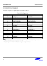
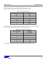
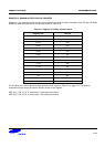
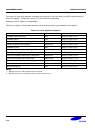
REGISTER 2: TRANSLATION TABLE BASE (TTB) REGISTER
This is the translation table base register, for the currently active first level translation table. The contents of register
2 are shown in Table 2-12.
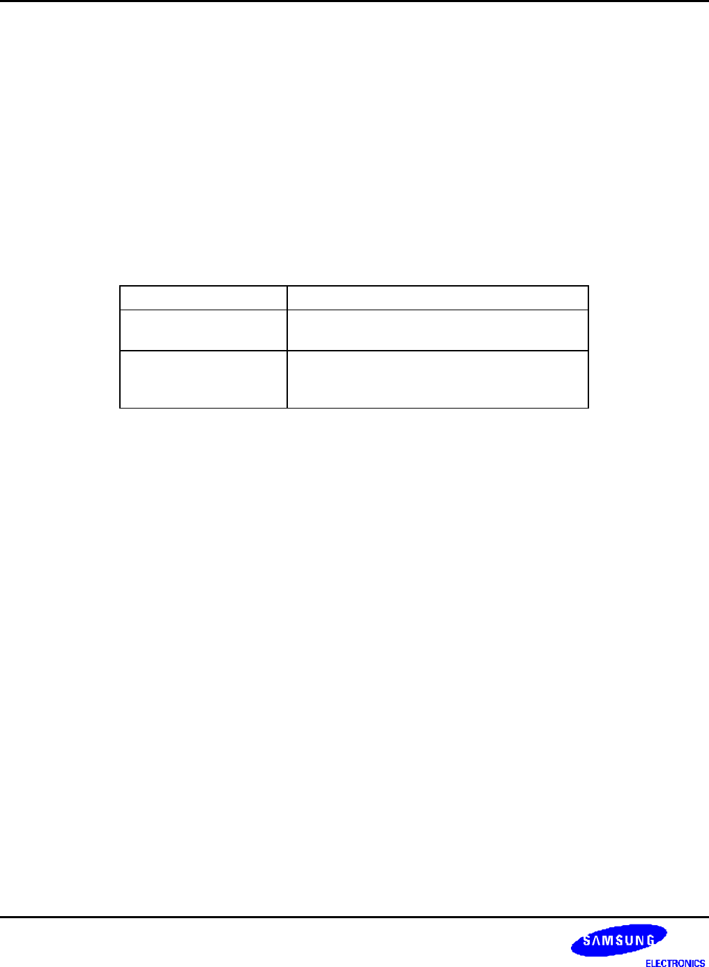
Table 2-12. Register 2: Translation Table Base
Register Bits Function
31:14 Pointer to first level translation table base.
Read/write
13:0 Reserved
Read = Unpredictable
Write = Should be zero
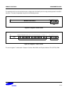
Reading from register 2 returns the pointer to the currently active first level translation table in bits[31:14]. Writing to
register 2 updates the pointer to the first level translation table from the value in bits[31:14] of the written value.
Bits[13:0] should be zero when written, and are unpredictable when read.
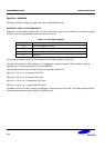
The following instructions can be used to access the TTB:
MRC p15, 0, Rd, c2, c0, 0; read TTB register
MCR p15, 0, Rd, c2, c0, 0; write TTB register